- 您现在的位置:买卖IC网 > Sheet目录342 > MIC2289C-34YD6 TR (Micrel Inc)IC LED DRIVR WHITE BCKLGT TSOT-6
Micrel, Inc.
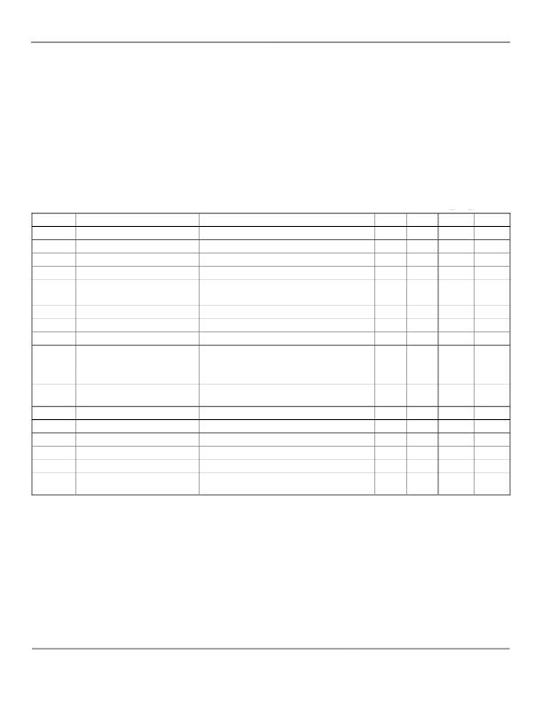
Absolute Maximum Ratings (1)
Supply Voltage (V IN ) .......................................................12V
Switch Voltage (V SW )....................................... –0.3V to 34V
Enable Pin Voltage (V EN )................................... –0.3V to V IN
FB Voltage (V FB )...............................................................6V
Switch Current (I SW ) .........................................................2A
Ambient Storage Temperature (T s ) ........... –65°C to +150°C
Schottky Reverse Voltage (V DA ).....................................34V
EDS Rating (3) .................................................................. 2kV
MIC2289C
Operating Ratings (2)
Supply voltage (V IN ) ........................................ 2.5V to +10V
Output Voltage (V IN ) ............................................ V IN to V OVP
Junction Temperature (T J ) ........................ –40°C to +125°C
Package Thermal Resistance
Thin SOT-23-6 ( θ JA ) ........................................177°C/W
Electrical Characteristics (4)
T A = 25°C, V IN = V EN = 3.6V, V OUT = 10V, I OUT = 20mA, unless otherwise noted. Bold values indicate –40°C< T J < +125°C.
Symbol
V IN
Parameter
Supply Voltage Range
Condition
Min
2.5
Typ
Max
10
Units
V
V UVLO
I VIN
I SD
Under Voltage Lockout
Quiescent Current
Shutdown Current
V FB > 200mV, (not switching)
V EN = 0V (5)
1.8
2.1
2.5
0.1
2.4
5
1
V
mA
μA
V FB
I FB
Feedback Voltage
Feedback Input Current
(±10%)
V FB = 95mV
85
95
–450
105
mV
nA
Line Regulation (6)
3V ≤ V IN ≤ 5V
0.5
%
Load Regulation
(6)
5mA ≤ I OUT ≤ 20mA
0.5
%
D MAX
I SW
V SW
Maximum Duty Cycle
Switch Current Limit
Switch Saturation Voltage
I SW = 0.5A
85
90
750
450
%
mA
mV
I SW
V EN
I EN
Switch Leakage Current
Enable Threshold
Enable Pin Current
V EN = 0V, V SW = 10V
TURN ON
TURN OFF
V EN = 10V
1.5
0.01
20
5
0.4
40
μA
V
V
μA
f SW
V D
I RD
Oscillator Frequency
Schottky Forward Drop
Schottky Leakage Current
I D = 150mA
V R = 30V
1.05
1.2
0.8
1.35
1
4
MHz
V
μA
V OVP
T J
Overvoltage Protection
Overtemperature
Threshold Shutdown
MIC2289C-34YD6 only
Hysteresis
27
32
150
10
37
V
°C
°C
Notes:
1. Absolute maximum ratings indicate limits beyond which damage to the component may occur. Electrical speci ? cations do not apply when operating
the device outside of its operating ratings. The maximum allowable power dissipation is a function of the maximum junction temperature, T J(max) , the
junction-to-ambient thermal resistance, θ JA , and the ambient temperature, T A . The maximum allowable power dissipation will result in excessive die
temperature, and the regulator will go into thermal shutdown.
2. The device is not guaranteed to function outside its operating rating.
3. Devices are ESD sensitive. Handling precautions recommended. Human body model.
4. Specification for packaged product only.
5. I SD = I VIN .
6. Guaranteed by design
August 2007
3
M9999-081507-B
发布紧急采购,3分钟左右您将得到回复。
相关PDF资料
MIC2291YD5 TR
IC LED DRIVER PHOTO FLASH TSOT-5
MIC2293-15YML TR
IC LED DRIVER WHITE BCKLGT 8-MLF
MIC2293C-34YML TR
IC LED DRIVER WHITE BCKLGT 8-MLF
MIC2297-42YML TR
IC LED DRIVR WHITE BCKLGT 10-MLF
MIC2298-15YML TR
IC LED DRIVER HIGH BRIGHT 12-MLF
MIC2299-15YML TR
IC LED DRIVR WHITE BCKLGT 12-MLF
MIC26603YJL EV
BOARD EVAL FOR MIC26603YJL
MIC26901YJL EV
BOARD EVAL FOR MIC26901YJL
相关代理商/技术参数
MIC2289C-34YML
制造商:MICREL 制造商全称:Micrel Semiconductor 功能描述:White LED Driver Internal Schottky Diode and OVP
MIC2289CBD5
制造商:MICREL 制造商全称:Micrel Semiconductor 功能描述:White LED Driver Internal Schottky Diode and OVP
MIC2289CYD5
制造商:MICREL 制造商全称:Micrel Semiconductor 功能描述:White LED Driver Internal Schottky Diode and OVP
MIC2290
制造商:MICREL 制造商全称:Micrel Semiconductor 功能描述:2mm 】 2mm PWM Boost Regulator with Internal Schotty Diode
MIC2290_07
制造商:MICREL 制造商全称:Micrel Semiconductor 功能描述:2mm 】 2mm PWM Boost Regulator with Internal Schotty Diode
MIC2290BML
制造商:MICREL 制造商全称:Micrel Semiconductor 功能描述:2mm 】 2mm PWM Boost Regulator with Internal Schotty Diode
MIC2290BML TR
功能描述:IC REG BOOST ADJ 0.5A 8MLF RoHS:否 类别:集成电路 (IC) >> PMIC - 稳压器 - DC DC 开关稳压器 系列:- 标准包装:20 系列:SIMPLE SWITCHER® 类型:降压(降压) 输出类型:固定 输出数:1 输出电压:12V 输入电压:4 V ~ 60 V PWM 型:电压模式 频率 - 开关:52kHz 电流 - 输出:1A 同步整流器:无 工作温度:-40°C ~ 125°C 安装类型:通孔 封装/外壳:16-DIP(0.300",7.62mm) 包装:管件 供应商设备封装:16-DIP 其它名称:*LM2575HVN-12LM2575HVN-12
MIC2290YML
制造商:MICREL 制造商全称:Micrel Semiconductor 功能描述:2mm 】 2mm PWM Boost Regulator with Internal Schotty Diode
